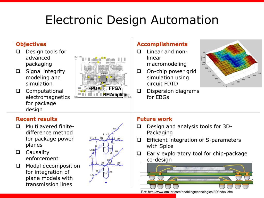
Electronic Design Automation: Revolutionizing Modern Electronics
In the intricate world of modern technology, where every device, from your smartphone to a complex medical scanner, relies on sophisticated electronic circuits, a silent revolution has been underway for decades. This revolution is powered by Electronic Design Automation (EDA). More than just a collection of software, EDA represents a critical market segment encompassing specialized software, sophisticated hardware, and essential services, all working in concert to define, plan, design, implement, and verify the electronic systems that underpin our digital lives.
At its core, Electronic Design Automation is the indispensable suite of tools and methodologies that enables engineers to transform abstract ideas into tangible, high-performing electronic products. It's the bridge between a conceptual circuit diagram and a manufactured integrated circuit (IC) or printed circuit board (PCB). Without EDA, the complexity of today's chips, housing billions of transistors, would be utterly insurmountable, making the rapid pace of technological innovation we've come to expect simply impossible.
What Exactly is Electronic Design Automation (EDA)?
Electronic Design Automation (EDA) is fundamentally the use of computer programs and specialized computer hardware to design, simulate, verify, manufacture, and test electronic systems. It’s a comprehensive set of software and hardware tools specifically engineered to assist in the entire lifecycle of electronic product development. From the earliest conceptualization to the final testing of a physical chip, EDA tools provide the necessary capabilities to handle the immense complexity involved.
Broadly encompassing the usage of software tools to develop or create electronic products, like integrated circuits (ICs) and printed circuit boards (PCBs), EDA has become the backbone of the semiconductor industry. In essence, it streamlines the design process, simulation, and validation of electronic circuits and systems, making it possible to create devices that are smaller, faster, more power-efficient, and incredibly complex. Without this sophisticated automation, the sheer scale of modern chip design, often involving billions of transistors, would be an impossible feat for human designers alone.
The Historical Evolution of EDA: From Manual Drafts to Digital Dominance
To truly appreciate the power of Electronic Design Automation, one must look back at its origins. In the past, hardware architects used to sketch circuit designs manually. This involved drawing schematics on paper, meticulously laying out components, and routing connections by hand. For simple circuits, this was manageable, but as electronics grew in complexity, so did the challenges. Errors were frequent, corrections were time-consuming, and verifying functionality was an arduous, often iterative, process involving physical prototypes.
The genesis of EDA can be traced back to the 1960s and 70s, driven by the increasing complexity of integrated circuits. Early tools were rudimentary, focusing on automating specific tasks like schematic capture or basic layout. The real breakthrough came with the advent of very-large-scale integration (VLSI) in the 1980s, which made it possible to integrate millions of transistors onto a single chip. This explosion in complexity necessitated a more robust and integrated approach to design, leading to the rapid development of what we now recognize as modern Electronic Design Automation. Companies like Cadence Design Systems, Synopsys, and Siemens EDA (formerly Mentor Graphics) emerged as pioneers, building comprehensive suites of tools that transformed the industry. This evolution from manual drafting to highly automated digital design has been nothing short of revolutionary, fundamentally changing how engineers approach electronic system development.
Why Electronic Design Automation is Indispensable Today
The question, "What is Electronic Design Automation (EDA), and why do you need it?" is answered by the sheer scale and demand of modern electronics. Today, the world runs on semiconductors. From the processors in our data centers to the tiny chips in our smartwatches, electronic systems are ubiquitous and increasingly complex. Without EDA, designing these systems would be economically unfeasible and practically impossible.
Here's why Electronic Design Automation is not just beneficial, but absolutely indispensable:
- Managing Complexity: Modern chips can contain billions of transistors. Manually designing, verifying, and optimizing such systems is beyond human capability. EDA tools automate repetitive tasks, manage vast datasets, and provide sophisticated algorithms to handle intricate design rules and interdependencies.
- Accelerating Time-to-Market: In the fast-paced electronics industry, being first to market can determine success. EDA significantly reduces design cycles, allowing companies to bring new products to consumers much faster.
- Ensuring Reliability and Performance: Errors in chip design can lead to catastrophic failures, costly recalls, and even endanger lives (in YMYL applications like medical devices or automotive systems). EDA tools provide rigorous simulation and verification capabilities, identifying potential issues long before manufacturing, thereby ensuring the reliability and optimal performance of the final product.
- Optimizing Cost and Power: EDA tools offer advanced optimization features that help engineers reduce chip size, minimize power consumption, and improve manufacturing yield, all of which directly impact the cost-effectiveness and environmental footprint of electronic devices.
- Facilitating Innovation: By abstracting away much of the low-level complexity, EDA allows engineers to focus on higher-level architectural innovation and explore new design paradigms, pushing the boundaries of what's possible in electronics.
Core Components and Tools within the EDA Ecosystem
Electronic Design Automation encompasses a suite of software tools used to design, simulate, and validate electronic circuits, systems, and devices. These tools are typically categorized by the specific stage of the design flow they address. Understanding these core components is key to grasping the holistic power of EDA.
Schematic Capture and Circuit Design
This is often the starting point of any electronic design. Schematic capture tools allow engineers to visually represent electronic circuits using standard symbols for components (resistors, capacitors, transistors, logic gates, etc.) and connections. These tools are crucial for translating an abstract idea into a structured, readable circuit diagram. They provide libraries of standard components, enable hierarchical design (breaking down complex systems into smaller, manageable blocks), and perform basic design rule checks to ensure connectivity and proper component usage. This foundational step is where the logical functionality of the circuit is defined.
Simulation and Verification
Once a schematic is drawn, the next critical step is to ensure it will behave as expected. Simulation tools allow engineers to test the circuit's functionality virtually, before any physical hardware is built. This includes:
- Circuit Simulators (e.g., SPICE): For analog and mixed-signal circuits, these tools predict voltage, current, and timing responses.
- Logic Simulators: For digital circuits, these verify the logical correctness of the design by simulating how signals propagate through gates and registers.
- Hardware Description Languages (HDLs) (e.g., VHDL, Verilog): These programming languages allow engineers to describe complex digital circuits at a higher level of abstraction, which can then be simulated and synthesized.
- Formal Verification: This advanced technique uses mathematical methods to rigorously prove the correctness of a design, ensuring it meets its specifications under all possible conditions, which is vital for YMYL applications.
- Emulation and Prototyping: For extremely complex systems, hardware emulators or FPGA-based prototypes can be used to run software on the designed hardware long before the actual chip is manufactured, accelerating software development and system-level verification.
These simulation and verification steps are paramount for identifying and correcting design flaws early, saving immense time and cost associated with physical prototyping and re-spins.
Physical Design and Layout
After the logical design is verified, it must be translated into a physical layout suitable for manufacturing. This phase is highly automated by EDA tools and includes:
- Synthesis: For digital designs, synthesis tools convert the HDL description into a gate-level netlist (a list of basic logic gates and their connections).
- Floorplanning: Determining the overall layout and placement of major functional blocks on the chip.
- Placement: Arranging individual logic gates and components on the chip.
- Routing: Connecting all the placed components with metal wires, ensuring signal integrity and adherence to manufacturing rules.
- Design Rule Checking (DRC): Verifying that the physical layout adheres to the foundry's manufacturing rules (e.g., minimum wire width, spacing).
- Layout Versus Schematic (LVS): Comparing the physical layout against the original schematic to ensure they are functionally identical.
This stage is incredibly complex, as it involves optimizing for performance, power, area, and manufacturability simultaneously. Modern EDA tools employ sophisticated algorithms, often leveraging AI and machine learning, to solve these multi-objective optimization problems.
Manufacturing and Test Preparation
The final stage of the design flow involves preparing the design for fabrication and ensuring it can be tested effectively. EDA tools assist here by:
- Generating GDSII/OASIS Files: These are the standard formats used by foundries to fabricate the chip masks.
- Test Pattern Generation (ATG): Creating a set of test vectors that can be applied to the manufactured chip to detect manufacturing defects. This often involves inserting Design-for-Test (DFT) structures into the chip during the physical design phase to make it more testable.
- Yield Analysis: Tools that help predict and improve the percentage of functional chips produced from a wafer.
This comprehensive suite of tools ensures that the design is not only functional but also manufacturable and testable at scale, directly impacting the economic viability of electronic products.
The EDA Workflow: A Journey from Concept to Chip
The Electronic Design Automation workflow is a highly structured, multi-stage process that guides engineers from an initial concept to a final, manufacturable design. While specific steps can vary depending on the complexity of the project (e.g., ASIC vs. FPGA vs. PCB), the general flow remains consistent.
It typically begins with high-level specification and architectural definition, where the desired functionality and performance targets are established. This is followed by logical design, which involves schematic capture or writing HDL code to describe the circuit's behavior. Once the logical design is complete, extensive simulation and verification are performed to ensure functional correctness. This iterative process of design and verification is crucial, often consuming the majority of the design cycle.
Upon successful verification, the design moves into the physical design phase. For integrated circuits, this involves synthesis, floorplanning, placement, and routing, transforming the logical design into a physical layout on silicon. For printed circuit boards, this involves component placement and trace routing on the board layers. Throughout this physical design stage, rigorous design rule checking (DRC) and layout versus schematic (LVS) checks are performed to ensure manufacturability and fidelity to the original design.
Finally, the design is prepared for manufacturing, generating the necessary data files (like GDSII for ICs) and test patterns to ensure the fabricated chips or PCBs are functional and defect-free. This systematic approach, heavily reliant on Electronic Design Automation software, streamlines the entire process, minimizing errors and accelerating the journey from a conceptual idea to a market-ready electronic product.
Key Benefits of Adopting Electronic Design Automation
The adoption of Electronic Design Automation has revolutionized the way engineers design and realize electronic systems, bringing forth a multitude of benefits that are critical for success in today's competitive landscape.
Perhaps the most significant benefit is the ability to handle unprecedented levels of complexity. As chips grow exponentially more intricate, with billions of transistors, manual design is simply not an option. EDA tools automate and manage this complexity, allowing engineers to focus on innovation rather than tedious, error-prone tasks. This automation directly translates into reduced design errors and significantly improved design quality, leading to more reliable and higher-performing products.
Furthermore, EDA dramatically accelerates the time-to-market. By streamlining every step from schematic capture to simulation, verification, and physical layout, companies can develop and release new products much faster than ever before. This agility is crucial in industries where product lifecycles are short and being first to market can confer a significant competitive advantage.
Cost reduction is another major advantage. While EDA software itself represents a significant investment, it pays for itself by minimizing the need for expensive physical prototypes, reducing design iterations (known as "re-spins"), and optimizing for manufacturing yield. The ability to simulate and verify designs thoroughly before fabrication saves millions in potential manufacturing errors and delays. Moreover, EDA tools aid in optimizing power consumption and chip area, leading to more efficient and cost-effective final products.
Finally, Electronic Design Automation fosters innovation. By providing powerful tools that abstract away low-level details, engineers are empowered to explore more complex architectures, experiment with novel circuit designs, and push the boundaries of what's electronically possible. This continuous cycle of innovation, driven by advanced EDA capabilities, is what propels the entire electronics industry forward.
Challenges and Future Trends in Electronic Design Automation
Despite its transformative power, the field of Electronic Design Automation is not without its challenges, and it continues to evolve rapidly to meet the demands of emerging technologies.
One of the foremost challenges is the ever-increasing complexity of designs, driven by Moore's Law and the demand for more functionality in smaller packages. Designing chips with trillions of transistors, integrating diverse functionalities (e.g., AI accelerators, RF, memory) onto a single die (System-on-Chip or SoC), and managing the thermal and power integrity of these systems pushes EDA tools to their limits.
Another significant hurdle is the rising cost of EDA licenses and the specialized expertise required to effectively utilize these sophisticated tools. As designs become more specialized, so too do the tools, demanding highly skilled engineers.
Looking ahead, several key trends are shaping the future of Electronic Design Automation:
- Artificial Intelligence and Machine Learning (AI/ML): AI and ML are increasingly being integrated into EDA tools to optimize various design stages, from intelligent floorplanning and routing to faster verification and power optimization. These techniques can find solutions that human designers might miss, significantly reducing design time and improving quality.
- Cloud-Based EDA: The computational demands of EDA are immense. Cloud computing offers scalable resources, allowing smaller companies to access powerful tools without massive upfront infrastructure investments. This trend is accelerating, offering greater flexibility and collaboration.
- Heterogeneous Integration and Advanced Packaging: Beyond traditional 2D scaling, the industry is moving towards 3D stacking of chips (chiplets) and advanced packaging techniques. EDA tools must evolve to handle the design and verification challenges of these multi-die systems, including inter-die communication, thermal management, and power delivery.
- Security and Trustworthiness: As electronics become more pervasive and critical, ensuring the security and trustworthiness of hardware designs is paramount. Future EDA tools will need to incorporate features for hardware security verification, IP protection, and supply chain integrity.
- Domain-Specific Architectures: With the slowing of general-purpose processor performance gains, there's a growing focus on designing highly specialized chips for specific applications (e.g., AI, automotive, IoT). EDA tools will need to adapt to support these highly customized design flows and verification methodologies.
These challenges and trends underscore the dynamic nature of EDA, which continuously innovates to remain at the forefront of technological progress.
Choosing the Right EDA Solutions: A Strategic Imperative
For any company involved in electronic product development, selecting the appropriate Electronic Design Automation solutions is a strategic imperative that can significantly impact success. The choice is not merely about acquiring software; it's about investing in a foundational capability that will shape product quality, development timelines, and overall competitiveness.
Major players in the EDA market include companies like Cadence Design Systems, Synopsys, and Siemens EDA (formerly Mentor Graphics), each offering comprehensive suites of tools covering the entire design flow. Beyond these industry giants, specialized vendors also provide niche solutions for specific tasks or design domains. For instance, Autodesk, known for its design software, offers solutions like Autodesk Fusion's advanced tools for PCB design, simulation, and verification, which streamline workflows for designers working on printed circuit boards.
When choosing EDA solutions, several factors must be considered:
- Design Requirements: What kind of electronics are being designed (ICs, PCBs, FPGAs, mixed-signal, RF)? The complexity and specific needs of the target designs will dictate the required tool capabilities.
- Integration and Workflow: How well do the chosen tools integrate with each other and with existing design flows? A seamless workflow minimizes manual data transfer and potential errors.
- Scalability: Can the tools handle future design complexity and larger projects? Scalability in terms of computational power and feature set is crucial for long-term investment.
- Vendor Support and Ecosystem: The quality of technical support, availability of training, and the broader ecosystem (e.g., IP libraries, foundry relationships) offered by the vendor are vital.
- Cost and Licensing Models: EDA software can be expensive. Understanding the licensing models (perpetual, subscription, cloud-based) and the total cost of ownership is essential.
- Industry Standards and Compatibility: Ensuring compatibility with industry-standard file formats (e.g., GDSII, Verilog, VHDL) and foundry processes is non-negotiable.
Ultimately, the right Electronic Design Automation solution is one that empowers engineers to efficiently and reliably bring their most innovative electronic designs to life, ensuring both technical excellence and market success.
In conclusion, Electronic Design Automation (EDA) is far more than just a collection of software tools; it is the fundamental enabler of modern electronics. From its humble beginnings in manual drafting to its current sophisticated state, EDA has consistently evolved to meet the escalating demands of complexity, performance, and time-to-market in the semiconductor industry. It is the silent hero behind every smart device, every advanced computing system, and every piece of critical infrastructure that defines our digital age.
As we look to the future, with the advent of AI-driven design, cloud computing, and advanced packaging techniques, EDA will continue to push the boundaries of what's possible, ensuring that the next generation of electronic innovations can be conceived, designed, and brought to life. Understanding EDA is not just for engineers; it's for anyone who seeks to grasp the foundational technology driving our world.
What are your thoughts on the future of Electronic Design Automation? Share your insights in the comments below! If you found this article informative, consider sharing it with your network or exploring other related articles on our site.
- Original Italian Pizza
- Peggy Martin Climbing Rose
- Suncoast Community Health Center
- Incredible Hulk Grey Hulk
- Olivia Brown
PPT - Electronic Design Automation PowerPoint Presentation, free

Electronic Design Automation - EDA - eVision Systems GmbH
什么是电子设计自动化 (EDA)? – 工作原理 | 新思科技
